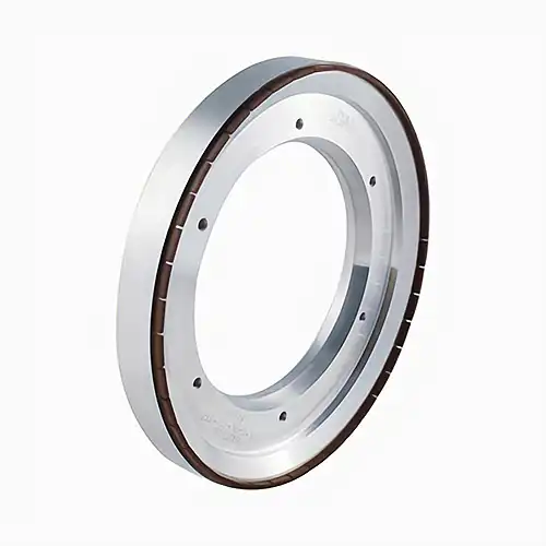
Wafer back grinding refers to control the thickness of the wafer within a certain range by wafer back grinding wheel. The main purpose is to meet the requirements of subsequent packaging processes, as well as the physical strength, heat dissipation, and size requirements of the chip. The integrity of the wafer is reflected in its absence of damage. Of course, during the wafer grinding process, it is inevitable that there will be wafer breakage.How to avoid wafer subsurface cracks of back grinding
Of course, during the wafer grinding process, it is inevitable that there will be wafer breakage.How to avoid wafer subsurface cracks of back grinding
Two Stages Of Wafer Grinding
fIrist Stage : Rough Grinding
The back grinding wheel will be used in this stage, and the abrasive particles of wheel are relatively coarse, with a large feed rate per revolution, and the cutting depth of a single abrasive particle is larger than the critical cutting depth. It is a typical brittle domain grinding.
The relatively high feed rate is used to improve processing efficiency, which accounts for about 94% of the total thinning amount in this stage. However, this process can cause significant lattice damage and edge chipping.

Second Stage: Fine Grinding
The diamond grinding wheel used in this stage has finer abrasive grains and a smaller feed rate per revolution, with some abrasive grains having a cutting depth less than the critical cutting depth. It belongs to ductile cutting. The cutting depth of the other part is larger than the critical cutting depth, which belongs to brittle domain grinding.
The lower feed rate is mainly used for eliminating damage, chipping, etc. Caused by rough grinding in the previous stage, accounting for 6% of the total grinding amount.

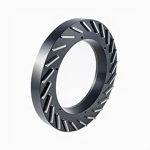
Quality Requirements For Wafer Grinding
Consistency requirements for wafer thickness
Surface Damage Layer Thickness (SSD) Requirements for Wafer
Surface roughness requirements for wafers
Requirements for TTV value of wafer surface thickness deviation
Requirements for wafer thickness accuracy and ultra-thin capability
Wafer integrity
The Integrity Of The Wafer Is Mainly Manifested In The Absence Of Damage To The Wafer
In the process of wafer grinding, there are many factors that can cause wafer subsurface cracks of back grinding. To reduce the probability of damage, it is necessary to start from the phenomenon and find the cause.
Three Forms Of Wafer Breakage
Crack Along The Direction Of The Abrasion.
‘Grinding marks’ refer to the grinding marks on the back of the wafer. This type of damage occurs on this abrasion mark.

Crack Along The Grain Path Of Wafer Subsurface Cracks of Back Grinding
Cracks occur linearly along the crystal direction. In rare cases, fracture does not occur along the crystal orientation, but this type of fracture is usually characterized by linear cracks.

Irregular Damage Of Wafer Subsurface Cracks of Back Grinding
It refers to cracks unrelated to crystal orientation and saw marks as shown in the figure, or the situation where the wafer is divided into several pieces.

Three forms of solutions for wafer breakage
Crack Along The Direction Of the Abrasion Mark
The fracture along the grinding mark is mainly caused by grinding defects such as blockage of the diamond grinding wheel chip groove. When the grinding wheel grinds with detached abrasive particles, it can cause high strain on the wafer and lead to fracture. In recent trends, fracture along the wear marks often occurs when the wafer has a thick oxide film.
This may be due to the mismatch between the chip and the z1 axis grinding wheel (used for rough grinding), that is, the grinding ability of the z1 axis grinding wheel is insufficient. Therefore, replacing the grinding wheel with a stronger grinding ability is one of the more effective methods to prevent breakage.
Especially when the fine surface is ground to 200 μ m or smaller, the possibility of breakage caused by factors 3 or 4 increases.
Main factors and measures:
Factor 1: Insufficient grinding ability of Z1 axis grinding wheel (rough grinding) (when grinding wafers with thick oxide films, etc.)
Measure: Replace the grinding wheel with a higher grinding power (e.g. choose a larger particle size, choose a binder with higher grinding power)
Factor 2: Grinding defects caused by water leakage between the grinding wheel and the wheel seat.
Measure: Check the installation surface of the wheel seat. If there are any objects, they should be removed.

Factor 3: Grinding defects caused by block of the grinding wheel chip groove.
During the fine grinding process, uncut tape or cut fragments can easily come into contact with the grinding wheel, causing them to get stuck between the teeth of the wheel and potentially leading to blockage of the cutting groove
Measure: Remove objects from the chip groove or replace the diamond grinding wheel.
Factor 4: Grinding defects caused by dragging chip cracks at the edge of the chip. During the thin surface grinding process, cracks are prone to appear at the edge of the wafer. During the processing, shattered fragments may be sandwiched between the grinding wheel and the wafer.
Measure: Adjust (reduce) the flow rate of the wheel coolant.
Fragmentation Along The Crystal Direction
Main factors and measures:
In the case of fracture along the crystal direction, the fracture is usually not caused by the grinding wheel, but mainly by\ substances (usually referring to grinding debris). The common factors and measures are shown in the table below:
Factor 1:There are objects on the chuck workbench
Measure:Clean the surface of the chuck

Factor 2:Objects between the adhesive film and the silicon wafer
Measure:Replace the adhesive film
Factor 3:There are particles and objects stuck on the transfer pad
Measure:Clean transfer pad
Irregular fragmentation
Main factors and measures:
In the case of fracture along the crystal direction, the fracture is usually not caused by the grinding wheel, but mainly by\ substances (usually referring to grinding debris). The common factors and measures are shown in the table below:
Factor 1:Collision with peripheral machine components during wafer processing
Measure:
Check the situation and adjust the installation positions of surrounding components
Factor 2:Insufficient wafer strength (during thin surface grinding process)
Measure:
Replace scrapped pieces and repeat testing equipment
Factor 3:Introduction of objects
Measure:
Careful inspection of the wafer is required (e.g. searching for objects attached to the chuck)
When defective Wafer subsurface cracks of back grinding , it is necessary to carefully analyze and eliminate them, and investigate the specific causes.